Yes, like centres of jumping spider eyes...
Perhaps we could MAKE a target from it? Does anyone with a slide have some of the liquid sensor-cleaner, which dries on the sensor and peels away with the dust ?
It may yield a relief pattern we could use.
Substitute for the resolution test slide 3000
Moderators: rjlittlefield, ChrisR, Chris S., Pau

Or photoresist remover? I found a pdf which lists a bunch of nasty, and probably unobtainable (by us) substances. But it also suggests a 3% NaOH solution (drain unblocker) which is easily obtainable.ChrisR wrote:Yes, like centres of jumping spider eyes...
Perhaps we could MAKE a target from it? Does anyone with a slide have some of the liquid sensor-cleaner, which dries on the sensor and peels away with the dust ?
It may yield a relief pattern we could use.
http://www.microchemicals.com/technical ... emoval.pdf
I'd try it myself but my first 2 slides got lost in the post. Seller has been very helpful and despatched replacements though so I'll have a go when those arrive.
Edit: oops, sorry I crossed threads. I was referring to Rik's suggestion that the slide may still have photoresist on.
Last edited by Beatsy on Wed Feb 08, 2017 6:25 am, edited 1 time in total.
Hello Rik,
Concerning the dependency on the illumination, we could use the same thick diffuser in order to achieve the comparable results, couldn’t we?
Thank you in advance.
Best regards,
ADi
Would you be so kind as to explain the meaning of “for any sort of a standardized test”?”For our macro rigs, and especially for any sort of a standardized test, the chip is close to useless because its appearance depends so strongly on the illumination”
Concerning the dependency on the illumination, we could use the same thick diffuser in order to achieve the comparable results, couldn’t we?
Thank you in advance.
Best regards,
ADi
-
siliconGary
- Posts: 73
- Joined: Tue Oct 18, 2016 2:40 pm
- Location: Canada
- Contact:
-
rjlittlefield

- Site Admin
- Posts: 23625
- Joined: Tue Aug 01, 2006 8:34 am
- Location: Richland, Washington State, USA
- Contact:
In principle, that could certainly be done. Any system that can be reproduced accurately and operated reliably can be used to make comparisons.Adalbert wrote:Would you be so kind as to explain the meaning of “for any sort of a standardized test”?rjlittlefield wrote:For our macro rigs, and especially for any sort of a standardized test, the chip is close to useless because its appearance depends so strongly on the illumination”
Concerning the dependency on the illumination, we could use the same thick diffuser in order to achieve the comparable results, couldn’t we?
What I'm skeptical about is whether that can be done, in practice, with this target.
This shiny reflective target is much harder to work with than matte and transmission targets are.
With, say, a chrome-on-glass slide such as Edmund's high-resolution USAF 1951 target, it's dead simple to get reproducible results. With that, you just set up any sort of diffuse backlighting, maybe do some minimal stacking to get around curvature of field or slight misalignment, and you're good to go.
But with a shiny reflective target, you have to either use through-the-objective illumination which most people don't have, or you have to deal with the light bouncing in odd ways that perturb the image, and/or you have to tilt the target quite a bit and deal with that by stacking. The number of variables to be controlled goes way up, and if they're not controlled enough, then the results become suspect at best, misleading at worst.
My phrasing "close to useless" may be too strong. I would be delighted to see experiments showing results to the contrary.
In that direction, I'll mention that I've been able to set up positioning and illumination that essentially reproduces the episcopic brightfield appearance of block 36, but using ordinary around-the-objective illumination. The trick is to tilt the slide rather steeply, about 22 degrees off axis in my experiment, so that with a sufficiently broad light source, light can reflect off the target into all portions of the objective's entrance pupil. However, the exact setup that works well for block 36 does not work so well for some other blocks, which apparently have a different 3D structure. The change in appearance mimics certain lens aberrations, so caution is advised...
--Rik

Pardon me for asking. I bought one and I do happen to have an epi scope, so I can see all these lines. But I don't know how they work - Rik how did you know what those spacings are that you've added in blue on your enlarged portion of your screengrab?
My extreme-macro.co.uk site, a learning site. Your comments and input there would be gratefully appreciated.
-
rjlittlefield
- Site Admin
- Posts: 23625
- Joined: Tue Aug 01, 2006 8:34 am
- Location: Richland, Washington State, USA
- Contact:
I think I'm reacting to the uniform pink color of the dark regions. I'm not using any polarization and the pink color does not change with angle of illumination, so I can make sense of it as a layer of some light-absorbing material and not as thin-film interference. But I have not much knowledge of chip manufacture and no other experience viewing chips, so I would be delighted to hear other explanations by people who actually know what they're talking about.siliconGary wrote:Looking at the images it doesn't look like photoresist to me. I am pretty sure that is just a patterned aluminum film on silicon oxide on silicon. The texture in the brightfieqld shot definitely looks like sputtered aluminum to me.
So, what causes the pink?
--Rik
-
rjlittlefield
- Site Admin
- Posts: 23625
- Joined: Tue Aug 01, 2006 8:34 am
- Location: Richland, Washington State, USA
- Contact:
Here's a quick single frame capture to illustrate some of the things that I've been talking about in the last couple of posts.
This is shot with a Nikon 20X 210/0 objective on an uncalibrated setup, direct projection through a 1.4X teleconverter to an APS-C sensor. Illumination is with a single Jansjö lamp with tissue paper around its head, jammed up against the objective.
The whole frame:

Camera-resolution 100% crop:
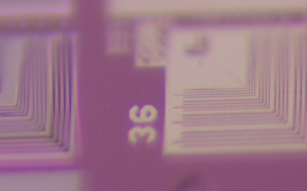
--Rik
This is shot with a Nikon 20X 210/0 objective on an uncalibrated setup, direct projection through a 1.4X teleconverter to an APS-C sensor. Illumination is with a single Jansjö lamp with tissue paper around its head, jammed up against the objective.
The whole frame:
Camera-resolution 100% crop:
--Rik
-
rjlittlefield
- Site Admin
- Posts: 23625
- Joined: Tue Aug 01, 2006 8:34 am
- Location: Richland, Washington State, USA
- Contact:
-
siliconGary
- Posts: 73
- Joined: Tue Oct 18, 2016 2:40 pm
- Location: Canada
- Contact:
Rik, the pink is the silicon oxide. Silicon oxide colour changes with thickness. Here is a colour chart of oxide thickness vs colour http://www.htelabs.com/appnotes/sio2_co ... ioxide.htmrjlittlefield wrote:I think I'm reacting to the uniform pink color of the dark regions. I'm not using any polarization and the pink color does not change with angle of illumination, so I can make sense of it as a layer of some light-absorbing material and not as thin-film interference. But I have not much knowledge of chip manufacture and no other experience viewing chips, so I would be delighted to hear other explanations by people who actually know what they're talking about.siliconGary wrote:Looking at the images it doesn't look like photoresist to me. I am pretty sure that is just a patterned aluminum film on silicon oxide on silicon. The texture in the brightfieqld shot definitely looks like sputtered aluminum to me.
So, what causes the pink?
--Rik
Typically you would not put an aluminum film directly onto the Silicon (When you etch the Aluminum pattern you would etch the silicon as well - whereas you can etch Aluminum and not the oxide - thus stop the etch on the oxide.)
An Aluminum film on silicon oxide test wafer is quite a common reference piece used for metrology in the wafer fabs. So that is what I think you have here. I would have thought it would have come with a diagram documenting the line pitches and patterns etc.
-
rjlittlefield
- Site Admin
- Posts: 23625
- Joined: Tue Aug 01, 2006 8:34 am
- Location: Richland, Washington State, USA
- Contact:
Gary, thanks for the explanation. I gather that the physics of the color is thin-film interference, but my intuition is wrong about how much the color will change with angle. The calculator at http://www.cleanroom.byu.edu/color_chart.phtml says that "the color generated by nitride or oxide on silicon films is heavily dependent on viewing angle", but playing with the calculator shows that a film of thickness 265 nm (2650 angstroms) film gives about the color that I'm seeing, with what I would consider only a modest change in color from 0 to 20 degrees.
Do I have that right?
--Rik
Do I have that right?
--Rik
-
siliconGary
- Posts: 73
- Joined: Tue Oct 18, 2016 2:40 pm
- Location: Canada
- Contact:
I don't recall how dependent on angle the colour is (I am a little surprised at the statement it is heavily dependent). There is a lot of repetition in the colour/thickness charts for similar colours. Unless you have specific instrumentation (Like a Nanometrics thin film interferometer) you kind of have to know what the approximate thickness is. You might be at 265nm, but you could also have 450-480nm and get similar colours.rjlittlefield wrote:Gary, thanks for the explanation. I gather that the physics of the color is thin-film interference, but my intuition is wrong about how much the color will change with angle. The calculator at http://www.cleanroom.byu.edu/color_chart.phtml says that "the color generated by nitride or oxide on silicon films is heavily dependent on viewing angle", but playing with the calculator shows that a film of thickness 265 nm (2650 angstroms) film gives about the color that I'm seeing, with what I would consider only a modest change in color from 0 to 20 degrees.
Do I have that right?
--Rik